Engineering-Design
From concept to production-ready package, we deliver complete electronic design solutions.
Schematics Design
A schematic is a visual representation of an electronic circuit, outlining the selected components and their connections. Our designers’ meticulous attention to detail and use of cutting-edge technologies ensure a high-quality end product tailored to your exact specifications.
Schematic Service:
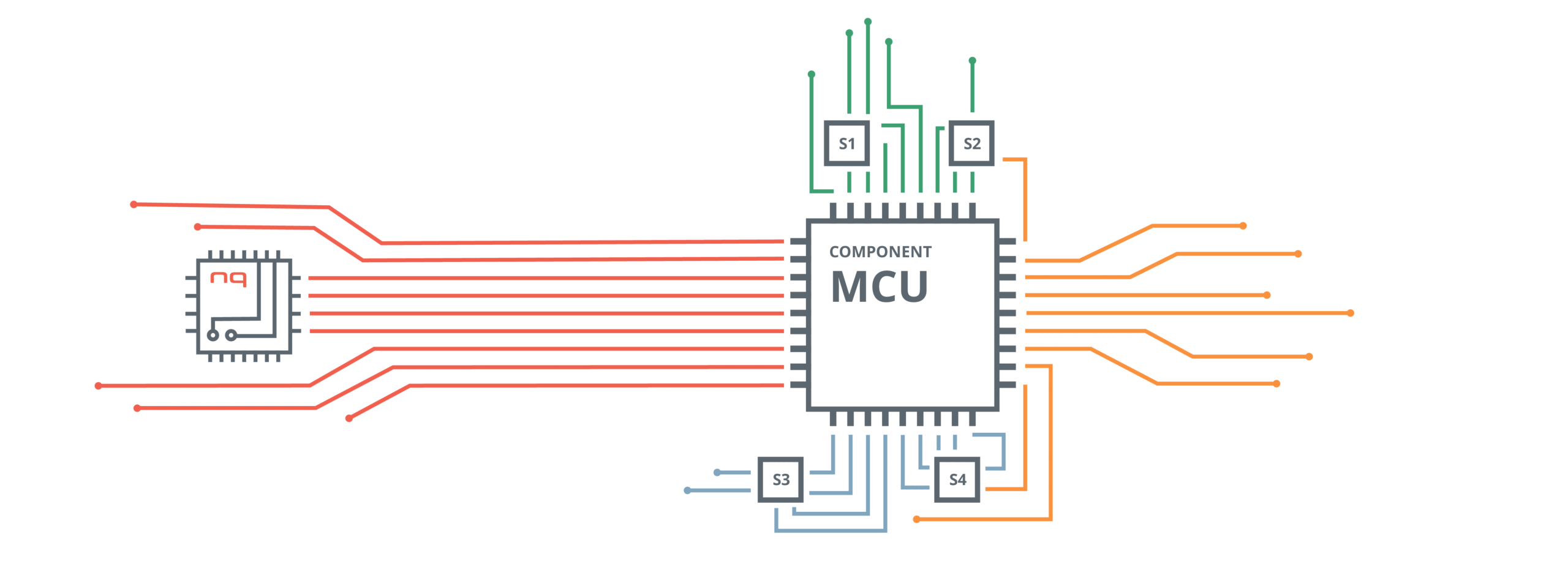
Schematics Capture
System Architectural Design
Conceptual Sketches
Component Selection
Smart PDF
Component Obsolescence Planning
System Block Diagram
Netlist Generation
Library Creation
We provide intelligent PCB library creation services, ensuring schematic symbols align with your library’s theme, including line width, naming conventions, pin assignments, colors, font preferences, and more. Our team works as an extension of yours, offering best practices and templates to maintain library consistency, reducing risk and downtime during manufacturing. Each schematic symbol undergoes a thorough preparation, review, and approval process to ensure the highest quality and accuracy, forming a solid foundation for your designs.

Categorized Components
Organized by type (resistors, capacitors, ICs, etc.).
Template-Based Symbols
Created from predefined templates for each component category.
Detailed Information
Includes part numbers, footprint, revision, polarity, and specific attributes.
3D Footprint Models
Visualize components in 3D for better design clarity.
Board Design
PCB Layout
PCB Layer Stack-up
Optimized copper and insulation arrangement for compact designs.
Multi-Layer PCB:
Designs with 2 to 32 layers for high-density applications.
Radio-Frequency PCB:
Supports wireless tech like Wi-Fi, Bluetooth, and LTE.
Design for Assembly:
Efficient component placement for smooth assembly.
Multi-Board PCB:
Integrated multiple boards for modular systems.
Heavy Copper PCB:
Over 4oz copper for power electronics and supplies.
Rigid-Flex PCB:
Mix of rigid and flexible layers for complex designs.
Flexible PCB:
Circuits that adapt to unique form factors.
High-Speed PCB:
Supports high-frequency interfaces for fast data transfer
High-Density PCB:
Compact designs with fine traces for more components.
Wireless Harness Design
An electrical wire harness is a system of cables arranged within insulation to transmit power or signals between devices, simplifying connections through a “drop-in” installation. Its design must meet the geometric and electrical needs of the equipment to ensure optimal performance.
The harness must be flexible and durable to withstand environmental and mechanical stresses like temperature extremes and vibrations, without interfering with the equipment’s function. After defining the design requirements, a schematic is created to produce manufacturing documentation, a bill of materials, and assembly instructions.
Electrical schematic creation from rough sketches or ideas
Component selection validation (fuses, relays, connectors, wires, terminations)
Bill of material generation
3D modeling of wire harness
Voltage drop, equipment, component, and cable sizing
Manufacturing packages
E4A Wire Harness Design Process
Gather system design requirements
Generate system block diagram and schematics
Produce bill of material, wire lists, and estimated cost
Develop prototype for testing and validation
Produce manufacturing, assembly, and test instructions
Design Package
Design package verification is a critical final step before PCB manufacturing, ensuring a comprehensive review of the design.
This includes checking footprints, routing constraints, controlled impedance, antenna and RF path design, component clearances, and optimized ground planes.
Once approved by the customer, we prepare a comprehensive Design Package for manufacturing, which includes the following essential files.
Design Package Contents
- Marketing Requirement Details
- Product Requirements Details
- Schematic Design
- Schematic in smart PDF format
- Complete bill of material
- Layout Design
- 3D model of PCB layout
- Design Rule Check confirmation
- Mechanical Constraints
- Gerber Files
- ODB++ Files
- Assembly drawings
- Pick and Place Files
- PCB Parasolid, DXF, and .STEP files


We're Here To Help!
Headquarters
Electronics4All
250 Herzberg Road
Ottawa, ON K2K 2A1
Lab Testing Facility
Hours
Monday – Friday: 8:30AM – 5PM EST
Saturday – Sunday: Closed