Electrical Design
Library Creation
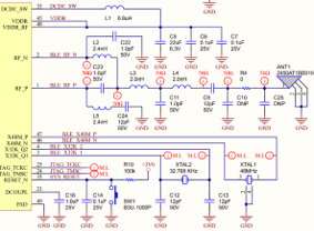
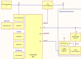
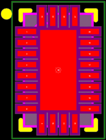
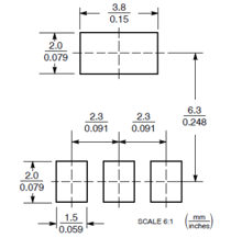
We offer intelligent PCB library creation services that generate schematic symbols that will fit your current library theme. This includes line width, naming convention, pins assignment, colors, pin length, font preferences, and many other attributes, which enables our team to work as an extension of your team. We also provide good practices and offer templates which can guarantee the consistency of your library, which is the foundation of any project to minimize risk and downtime during the manufacturing cycle.
Every schematic symbol goes through a prepare, review, and approval process to ensure the highest quality and accuracy of the symbol, as it serves as the foundation of customer’s designs.
Each of our schematic symbols contains the following attributes:
If you have a library that requires to be re-structured to make it more reliable, we can also retrofit your library to ensure it is accurate and consistent, and we can also maintain your library while your team focuses on your core business.
PCB Layout
Our Capabilities/What We Do
PCB Layer Stack-up:
Arrangement of copper and insulating layers that make up the PCB to optimize and enable more circuitry on a single board
Multi-Layer PCB:
High-density designs incorporating from 2 to 32 layers into a single PCB
Radio-Frequency PCB:
Wireless capability (Wi-Fi, Bluetooth, communication 900MHz, LTE, and others)
Design for Assembly:
Optimized PCB component placement, routing, and clearance to maximize product yield during product assembly
Multi-Board PCB:
Multiple PCBs connected to create one integrated design and provide modularity to a system
Heavy Copper PCB:
Finished copper weight of more than 4oz. used extensively in power electronic devices and power supply systems
Rigid-Flex PCB:
2+ conductive layers comprised of flexible and rigid insulation material for complex designs
Flexible PCB:
Flexible circuit boards enable circuitry to adapt to fit a specific product form factor
High-Speed PCB:
Digital frequency exceeding 50MHz, utilizing HDMI, SATA, Ethernet, or other high-speed interfaces for quick data transfer
High-Density PCB:
High circuit density with trace widths below 8mil, micro-vias, and blind/buried vias to reduce board size while increasing component count
Electronics4All uses the most current and trusted PCB design tools, and we can transfer your legacy files to the platform of your choice, including Altium Designer, Cadence OrCAD / Allegro, Protel 99, Eagle, or others.
Wire Harness Design
An electrical wire harness is an arrangement of cables within an insulated material in an organized and systematic manner. Its purpose is to transmit signal power or electrical power between two or more electrical devices and simplifies the connection to end components by integrating the wiring into a “drop-in” installation. During the design of a wire harness, consideration must be given to the geometric and electrical requirements of the equipment it is to be installed in to ensure the rigout output is generated.
The wire harness must be designed to be sufficiently flexible and durable to withstand the environmental and mechanical conditions of the equipment such as extreme temperature, temperature fluctuations, and vibration. The designer must also ensure that the harness does not interfere with the equipment’s performance. Once the wire harness design requirements are established, a schematic is created to generate the manufacturing documentation, bill of material, and assembly board for the harness.
Capabilities:
E4A Wire Harness Design Process
Design Packages
Design package verification is a critical step as it’s the final step prior to the manufacturing process of the PCB. This involves a complete review of the design, including the footprints, routing constraints, line length matching, controlled impedance, proper antenna design and RF path for wireless devices, component and board edge clearances, component height constraints, assembly constraints, optimized ground planes, and many others.
Once this review is complete and approved by the customer, we generate a Design Package ready for manufacturing that will include the following files at minimum:
